 As discussed in my MAX1241 project, there are a number of advantages for utilizing external analog to digital converters (ADCs) in a project’s design. The MAX144 is a 12-bit two-channel ADC that has a “7.4µs successive-approximation ADC, automatic power-down, fast wake-up (2.5µs), an on-chip clock, and a high-speed, 3-wire serial interface.” All of these contribute to a wonderful, fast, two-channel analog-to-digital converter, which can be utilized in a number of situations where high-speed (108ksps) data acquisition is necessary.
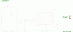
Full Circuit
The source and firmware for the circuit can be found at the bottom of the page. Each section of the circuit is labeled in the schematic. All of the sections and their components are described and discussed below. The part numbers for the components are linked to websites for data and more information when available.
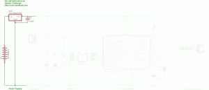
Power Supply
The power supply uses a 9 volt battery and a TC1262-5.0V high-accuracy low-dropout linear voltage regulator to provide a stable 5 volt supply for the microcontroller and the MAX144. A 1uF (microFarad) polarized decoupling capacitor is necessary on the output of the voltage regulator to prevent power spikes or ripples. A wall wart power supply as low as 5.3V can be substituted for the 9 Volt battery.
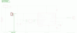
Analog Input
The analog input is connected to the A0 pin on the PIC, which is configured to be an analog input, and the CH0 and CH1 pins on the MAX144. Please note that for the PIC, “The source impedance affects the offset voltage at the analog input (due to pin leakage current). The maximum recommended impedance for analog sources is 2.5 kΩ” (PIC18F2550, pp. 260). In addition, please note that for the MAX144, “The acquisition time, tACQ, is the maximum time the device takes to acquire the signal, and is also the minimum time required for the signal to be acquired. Calculate this with the following equation: tACQ = 9(RS + RIN)CIN where RS is the source impedance of the input signal, RIN (9k) is the input resistance, and CIN (16pF) is the input capacitance of the ADC. Source impedances below 1k have no significant impact on the AC performance of the MAX144/MAX145” (MAX144, pp. 8).
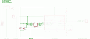
MAX144
The MAX144 is a “Low-power, 12-bit analog-to-digital converter (ADC) … [that operates] with a single +2.7V to +5.25V supply and features a 7.4μs successive-approximation ADC, automatic power-down, fast wake-up (2.5μs), an on-chip clock, and a high-speed, 3-wire serial interface” (MAX144, pp. 1). The bypass capacitors (C2 and C3) are necessary to minimize power input fluctuations.
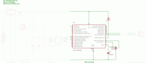
Microcontroller
The microcontroller used is a Microchip PIC18F2550. I modified the PIC18F2550 Tiny PIC Bootloader assembly file so I could use a 20MHz crystal/resonator at 115,200 baud (the modified bootloader can be found at the bottom of the page). The PIC18F2550 runs at 48MHz using the internal PLL. R1 is a pull-up resistor necessary for operation. C1 is a stabilizing capacitor that is used for the onboard USB voltage regulator, which is not used in this project. The component marked ‘RES’ is a 20MHz resonator.
RS232 Level Converter
The microcontroller USART pins need to be connected to a RS-232 Level Converter to connect to a PC for firmware updates using the Tiny PIC Bootloader. Otherwise, after initial programming they can be left disconnected.
Source and Firmware
The PIC must initially programmed with the ‘SAC_tinybld18F2550usb _20MHz_115200_48MHz’ hex file to program the bootloader on the PIC. Then, using Tiny PIC Bootloader, the hex file can be placed on the chip using the Tiny PIC Bootloader frontend with ’12h 34h 56h 78h 90h’ in the ‘List of codes to send first:’ in the ‘Options’ menu. Please feel free to contact me if you have any problems.
– SAC_tinybld18F2550usb_20MHz_115200_48MHz
– 18F2550 MAX144 SPI.c (hex)
– 18F2550 MAX144 int16.c (hex)
